 EASY
EASYJSS University Mysore Allied Sciences 2026
NAAC A+ Accredited| Ranked #21 in University Category by NIRF | Applications open for multiple UG & PG Programs


Characteristics of a P-N junction is considered one the most difficult concept.
Semiconductor Diode(I), Semiconductor Diode(II) is considered one of the most asked concept.
53 Questions around this concept.
If in a p-n junction, a square input signal of 10 V is applied, as shown,

then the output across RL will be:
Which one of the following represents the forward bias diode?
In forward biasing of the p-n junction
In the following figure, the diodes which are forward biased are
(a)
(b)
(c)
(d)
Assuming the diodes to be of silicon with forward resistance zero, the current I in the following circuit is

In the middle of the depletion layer of a reverse- biased junction, the
The V-I characteristic of a diode is shown in the figure. The ratio of forward to reverse bias resistance is :

When $p-n$ junction diode is forward biased, then
Two ideal diodes are connected to a battery as shown in the circuit. The current supplied by the battery is:

Consider the following statements A and B and identify the correct answer:
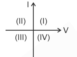
A. For a solar cell, the I-V characteristics lie in the IV quadrant of the given graph.
B. In a reverse biased PN junction diode, the current measured in ($\mu $A), is due to majority charge carriers.
Semiconductor diode-
If a p-n junction has metallic contacts at both the ends for application of external voltage. This is called a semiconductor diode.

The symbolical representation of a semiconductor diode is shown below -

In the figure given above, the arrow indicates the direction of current when the diode is under forward bias. One should note here that the equilibrium barrier potential can be altered. This can be done by applying an external voltage across the diode. Depending on how this voltage is applied, the diode is a forward-bias or a reverse-bias diode which we will study in the upcoming concept.
P-n junction diode under forward bias-

In the figure given above, we can see that an external voltage is applied across the semiconductor diode where the p-side of the diode is connected to the positive terminal and the n-side is connected to the negative terminal of the battery. This type of arrangement for the diode is forward biased.
Formation of a Forward Bias Diode-
As the depletion region have no charge so the resistance is very high there so the applied voltage drops primarily across this region. The drop in voltage across the p and n side of the junction is relatively negligible. And the direction of the applied voltage (V) being opposite to that of the built-in potential (Vo) due to which the depletion layer’s width decreases and the barrier height reduce.
If the applied voltage is small, then the barrier potential is reduced marginally only below the equilibrium value. Then only small number of carriers crossing the junction, so the current is small. Similarly for a significantly high value of voltage, more carriers have the energy to cross the junction so, the current will be high.
One should also note that when the voltage is applied, some electrons cross to the p-side and some holes cross to the n-side. Under forward bias, this process is the minority charge injection process. Hence, the minority charge concentration which is electrons on the p-side are a minority and holes on the n-side are a minority, is significantly higher at the junction boundary.

Due to this concentration gradient, the injected electron diffuse from the junction-end to the far-end of the p-side. Similarly, injected holes diffuse to the far end of the n-side. This gives rise to current too.
The total diode forward current = Hole diffusion current + Electron diffusion current (mA)
P-n junction diode under reverse bias-

In the figure given above, we can see that an external voltage is applied across the diode. We can see that the n-side of the diode connects to the positive terminal and the p-side connects to the negative terminal of the battery. This type of arrangement in diode is a reverse-bias diode.
Formation of a Reverse Bias Diode
As the depletion region have no charges, so the resistance will be very high, as a result the applied voltage drops primarily across this region. Also the drop in voltage across the p and n side of the junction is relatively negligible. Now here the direction of the applied voltage (V) being the same as that of the built-in potential (V0) (Opposite to the forward bias), because of this the depletion layer’s width widens and the barrier height also increases. This decreases the flow of electron to the p-side and holes to the n-side. So, the diffusion current decreases to a great extent.
Because of the direction of the electric field, the electrons in the p-side and holes in the n-side are drive to their majority zones, if they come close to the junction. This will produces the drift current. The drift current is usually of a few microAmprere. This current is very low even in the forward-biased diode as compared to the current due to the injected carriers.
Critical Value of Reverse Bias Voltage -
A small amount of voltage applied to the diode is sufficient to sweep the minority charge carrier to the far side of the junction. This diode reverses current which is not dependent on the voltage but on the concentration of the minority charge carriers on both sides of the junction. However, the current is independent up to a critical value of reverse bias voltage which is the Breakdown Voltage (Vbr). When the voltage applied crosses breakdown voltage i.e., Vbr, even a small change in the bias voltage causes a huge change in current. There is an upper limit of current for every diode, beyond which the diode gets destroyed due to overheating. This is the rated value of current.
Experimental Study of the V-I characteristics of a Semiconductor Diode

The figure shows a diode connected in reverse bias. The battery connects to the diode through a potentiometer by which we can change the voltage of the experiment. A microammeter is also used (since the expected current is in milliAmpere) measures the current.
Here is the result of the experiment

As we can see in the graph above, in the forward biased diode, initially when the current increases almost negligibly till a certain value is reached. After that, the current increases exponentially even for a small increase in diode bias voltage. This voltage is called as threshold voltage. (Its value is approximately ~0.7 V for silicon diode and ~ 0.2 V for germanium diode)
In the reverse biased diode, the current is very small and almost remains constant with a change in bias voltage. It is called as Reverse saturation current. It is observed that in some cases, beyond the breakdown voltage, the current increases suddenly.
Hence, from this experiment and the given graph, we can conclude that the p-n junction diode allows the flow of current only in one direction, i.e. forward-bias, which means that the forward bias resistance is lower than the reverse bias resistance.
Extra edge -
1. P -N junction as diode
R = 0, Forward
R = Reverse
It is a one way device. It offers a low resistance when forward biased and high resistance when reverse biased.
2. Dynamic Resistance
Since slope of potential vs current graph is non uniform hence resistance keep changing .
$R_d=\frac{d v}{d i}$

3. Knee voltage of P-N junction
Knee voltage for Ge is 0.3 V
Knee voltage for Si is 0.7 V
It is defined as that forward voltage at which the current through the junction starts rising rapidly with increase in voltage .
4. Relation between current I & Voltage V
K = Boltzmann constant
I0 = reverse saturation current
In forward bias
$$
e^{\frac{e v}{K T}} \gg 1
$$
Then forward biasing current is
$$
\begin{aligned}
& I=I_0 \cdot e^{\frac{c v}{K T}} \\
& I=I_0\left(e^{\frac{v}{K T}}-1\right)
\end{aligned}
$$
"Stay in the loop. Receive exam news, study resources, and expert advice!"
Recognized as Category 1 University by UGC | Accredited with A+ Grade by NAAC | Scholarships available
Ranked as India’s #1 Not for profit pvt. University by India Today
Ranked among the top Dental Colleges for 7 consecutive years by India Today poll
Get Started With Your Healthcare Career. 2026 Admissions open.
Get Job Ready in Healthcare | Employability-Focused Programs
Allied & Healthcare programs | 20+ Partner Universities & Institutes | 98% placement record