JSS University Mysore Allied Sciences 2026
NAAC A+ Accredited| Ranked #21 in University Category by NIRF | Applications open for multiple UG & PG Programs


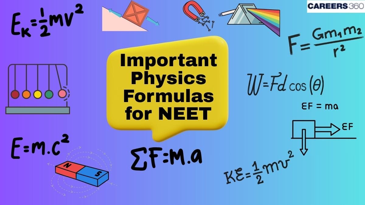
Preparing for NEET 2026 requires a strong command of Physics formulas, as many questions in the exam are based on direct formula application and numerical problem-solving. Revising important equations regularly helps improve accuracy, speed, and conceptual understanding. To make your preparation easier, we have compiled a topic-wise NEET 2026 Physics formulas sheet covering Mechanics, Thermodynamics, Electrostatics, Current Electricity, Modern Physics, Optics, and other high-weightage chapters.
This Story also Contains
Candidates can use this NEET Physics formula sheet PDF for quick revision during the final stages of preparation. Learning these formulas along with their applications can help students solve questions more efficiently and avoid common calculation errors in the NEET exam.
To make the NEET physics study easier for aspirants, all the important physics formulas for NEET 2026 are given in one place. It is prepared to help students revise quickly and solve questions with speed and accuracy. The formula sheet covers key topics from mechanics, thermodynamics, electricity, waves, and modern physics.
| Access to NEET Physics Important Formulas | Download NEET 2026 Physics Formula Sheet PDF (Free) |
Get expert advice on college selection, admission chances, and career path in a personalized counselling session.
The following formulas are arranged systematically to help candidates prepare the NEET Physics syllabus for NEET 2026 in an organised manner:
Displacement: $s = ut + \frac{1}{2}at^2$
Final velocity: $v = u + at$
Velocity–displacement relation: $v^2 = u^2 + 2as$
Average velocity: $v_{\text{avg}} = \frac{u + v}{2}$
Where:
u = initial velocity
v = final velocity
a = acceleration
t = time
s = displacement
Memory tip:
Start with v=u+at. Displacement grows as ut plus the extra part from acceleration.
Time of flight: $T = \frac{2u\sin\theta}{g}$
Maximum height: $H = \frac{u^2\sin^2\theta}{2g}$
Horizontal range: $R = \frac{u^2\sin 2\theta}{g}$
Where:
u = initial speed
θ = angle of projection
g = acceleration due to gravity
Time of flight: $T = \frac{2u\sin\theta}{g}$
Maximum height: $H = \frac{u^2\sin^2\theta}{2g}$
Horizontal range: $R = \frac{u^2\sin 2\theta}{g}$
Heat gained or lost: $Q = mc\Delta T$
Heat during phase change: $Q = mL$
Energy of photon: $E = h\nu$
Kinetic energy of emitted electron: $KE = h\nu - \phi$
Centripetal force: $F = \frac{mv^2}{r}$
Angular velocity: $\omega = \frac{v}{r}$
Time period: $T = \frac{2\pi r}{v}$
Voltage across resistor: $V_R = iR$
Voltage across inductor: $V_L = i\omega L$
Voltage across capacitor: $V_C = \frac{i}{\omega C}$
Impedance: $Z = \sqrt{R^2 + \left(\omega L - \frac{1}{\omega C}\right)^2}$
Phase angle: $\tan\phi = \frac{\omega L - \frac{1}{\omega C}}{R}$
Acceleration: $a = -\omega^2 x$
Displacement: $x = A\sin(\omega t + \phi)$
Velocity: $v = A\omega\cos(\omega t + \phi)$
Differential equation: $\frac{d^2x}{dt^2} + \omega^2 x = 0$
Conducting sphere (outside): $V = \frac{Q}{4\pi\varepsilon_0 r}$
Conducting sphere (inside): $V = \frac{Q}{4\pi\varepsilon_0 R}$
Non-conducting sphere (inside): $V = \frac{Q}{8\pi\varepsilon_0 R^3}\left(3R^2 - r^2\right)$
Resistance: $R = \rho \frac{l}{A}$
Resistivity: $\rho = \frac{m}{ne^2\tau}$
Kirchhoff's Voltage Law: $\sum V = 0$
Speed of light: $c = \frac{1}{\sqrt{\mu_0\varepsilon_0}}$
Relation between fields: $B = \frac{E}{c}$
Critical angle: $\sin C = \frac{n_2}{n_1}$
Young's Double Slit Experiment
Bright fringe: $x = \frac{n\lambda D}{d}$
Dark fringe: $x = \frac{(2n-1)\lambda D}{2d}$
Fringe width: $\beta = \frac{\lambda D}{d}$
$\lambda = \frac{h}{p}$
For electron accelerated through potential $V$: $\lambda = \frac{12.27}{\sqrt{V}}$
NOT gate: $Y = 1 - A$
AND gate: $Y = A \cdot B$
OR gate: $Y = A + B$
NAND gate: $Y = 1 - A \cdot B$
NOR gate: $Y = 1 - (A + B)$
Also read:
|
NEET 2026 Exam Analysis PDF: Difficulty Level, Student Reactions, Subject-Wise Paper Review | |
|
NEET 2026 Physics Answer Key with Solutions PDF – Download |
Flashcards are useful because they help you revise super fast and test yourself anytime, anywhere. You can flip through them on the bus, before sleeping, or even while waiting for tea, and that small effort adds up big time in your memory. Use these to keep important NEET physics formulas at your fingertips, no tension, no stress.
$v = u + at$ – First equation of motion
$s = ut + \frac{1}{2}at^2$ – Displacement
$F = ma$ – Newton’s second law
$W = Fd\cos\theta$ – Work done
$KE = \frac{1}{2}mv^2$ – Kinetic energy
$PE = mgh$ – Potential energy
$V = IR$ – Ohm’s law
$R = \rho \frac{l}{A}$ – Resistance
$\lambda = \frac{h}{mv}$ – De Broglie wavelength
$Q = mc\Delta T$ – Heat equation
Knowing some smart tricks to remember physics formulas is just as important as memorising them. When you use these little hacks, formulas stick better and come to you faster during exams. It saves time and keeps you calm under pressure. Starting early and revising regularly makes the whole preparation less stressful and way more effective. Here’s how to use the NEET Formula Sheet 2026 and remember formulas like a pro:
Start revising formulas from day one of your NEET exam preparation so you build a solid base right from the start.
Spend 10 to 15 minutes every day just going over the formula sheet to keep things fresh in your brain.
Don’t only memorise, understand the theory behind the formulas so you can apply them easily when needed.
Keep your formula sheet close while practising previous years' NEET questions. It helps connect theory with actual problems.
Make the sheet your own by adding quick notes or shortcuts that help you remember stuff faster during the exam.
Practice the top 50 physics numericals based on the important formulas to score 120+ marks
Frequently Asked Questions (FAQs)
You can download the Physics formula sheet for NEET 2026 PDF from this page. It includes all important formulas arranged chapter-wise for quick revision.
Revise the formula sheet daily and apply each formula using NEET PYQ chapterwise physics. This helps you understand real exam questions and improves accuracy.
Formulas are important, but you must also practice numericals and solve NEET chapterwise pyq regularly. Combining formulas with PYQs ensures better concept clarity and higher scores.
The Re-NEET 2026 exam is being conducted today. The question paper PDF will be made available as soon as the exam is over.

On Question asked by student community
Hello Dear Student,
With 407 marks and an AIR of 255910, your chances of securing a Government BAMS seat in Uttar Pradesh are very low. Government BAMS cut offs in UP generally close between 450 and 530 marks depending on your category.
You can check, find and access more information
You can watch recorded NEET counselling webinars from several trusted sources:
Medical Counselling Committee (MCC) – The official MCC website publishes counselling schedules, notices, information bulletins, and updates. While it does not regularly host recorded webinars, it is the most reliable source for official counselling information.
Hey there,
With 343 marks in NEET UG and Bihar domicile, getting an MBBS seat at Katihar Medical College through the mop-up or stray vacancy rounds is possible but not guaranteed. Admission depends on your NEET rank, category, counselling round, and seat availability. You should participate in all Bihar UGMAC
Hey there,
With 115 marks in Re-NEET 2026, getting a BAMS seat through the management quota is unlikely, as you must first qualify NEET and also meet the eligibility criteria prescribed by the counselling authority. If your score is above the official qualifying cutoff for your category, you may have
Hello Dear Student,
With 526 marks in the NEET 2026 exam, your expected All India Rank (AIR) will be roughly in the range of 26,000 to 39,000. For the OBC category specifically, your state rank in Bihar will likely hover between 4,000 and 6,000.
You can check, find and access
the product 'P' will be ,


| Column A | Column B |
| A |
a) Organisation of cellular contents and further cell growth. |
| B |
b) Leads to formation of two daughter cells. |
| C |
c) Cell grows physically and increase volume proteins,organells. |
| D |
d) synthesis and replication of DNA. |
Match the correct option as per the process shown in the
0.16 g of dibasic acid required 25 ml of decinormal solution for complete neutralisation. The modecular weight of the acid will be
32
64
128
256
0xone is
Register for iACST. Get instant Scholarship on NEET Repeater Courses.
Know possible Govt/Private MBBS/BDS Colleges based on your NEET rank
College Predictors Webinars One to One Counselling Regular Updates Medical Almanac
Alied Health Sciences at SCSVMV | NAAC 'A' Grade | AICTE & UGC Aproved | 100% Placement Support | Merit-based Scholarships
5+ Crore Scholarship for Meritorious Students | 250+ Recruiters | 10,000+ Placements | 20 Lakhs Highest Package
Highest Package: ₹32 LPA | Placement Rate: 90% students placed | 5000+ Students Placed 900+ Placements Recruiters | Scholarships Available